Printed circuit board surface finish
The circuit board surface is responsible for raising the wetting ability of the contact areas for soldering; non-chemical surfaces serve simultaneously as protection against oxidation of the covered copper and improve shelf life characteristics.
The circuit board surfaces vary in shelf life, typical application field and price, but are normally specified by the process, product or desired location for the application.
| Surface |  |  |  |  |  |  |  |  |  |  |  |  |
|---|---|---|---|---|---|---|---|---|---|---|---|---|
| Hal SnPb |  |  | >5µm | ca.12 months | 5 | |||||||
| HAL lead-free |  |  |  | >5µm | ca. 12 months | 5 | ||||||
| Chemical tin |  |  |  | >1µm | ca. 6 months | 5 | ||||||
| Chemical silver |  |  |  |  | 0.2 - 0.3µm | ca. 12 Monate | 5 | |||||
| Chemical gold ENIG |  |  |  |  |  |  | 3-6µm Ni 0.05-0.1µm Au | ca. 12 months | 5 | |||
| ENEPIG |  |  |  |  |  |  | 3-8µm Ni 0.05-0.15µm Pd 0.05-0.1µm Au | ca. 12 months | - | |||
| Galvanic softgold |  |  |  | 4 - 6µm Ni >1µm Au | ca. 12 months | - | ||||||
| Galvanic hardgold |  |  |  | 4 - 6µm Ni 0.1 - 2µm* Au | ca. 12 months on request | - |
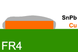
HAL SnPb (lead-tin) is nowadays allowed only in certain technology fields such as medicine and space travel. HAL is suitable for standard SMD, but shows weaknesses in fine pitch applications. A chemical surface is preferable for finepitch.

Advantages:
Good solderability
Good reflow properties
Disadvantages:
Pads are non-planar
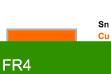
The surface chemical tin is for manufacturing reasons rarely requested any more! Due to the rapid oxidation of the copper, the shelf life is highly dependent on temperature and packaging. Fingerprints on the surface should be avoided at all.

Advantages:
Absolutely flat
Good for fine pitch
Good for SMD
Good for press-fit
Disadvantages:
Extra charge
Critical manufacturing process
Faster oxidation, thus:
Limited storability
Office: 803-804, Hisee International Commercial Center, Dongbin Road, Nanshan District, Shenzhen, China
Factory Add: 4/F, C2 Building, Hezhou, Hengfeng Industrial City, Xixiang Street, Bao'an District, Shenzhen, China